Modern UEFI bios rom capacity serves as the foundational constraint for system initialization within the global cloud and network infrastructure stack. Unlike legacy BIOS systems that resided within 512 KB to 1 MB of Electrically Erasable Programmable Read-Only Memory (EEPROM), modern UEFI firmware typically necessitates between 16 MB and 64 MB of Serial Peripheral Interface (SPI) flash storage. This increase in capacity is driven by the requirement for more complex encapsulation of hardware drivers; extensive microcode updates for multi-core processors; and sophisticated pre-boot execution environments. In high-density data centers, the UEFI bios rom capacity governs the ability of a node to support diverse operating system payloads and high-speed networking protocols before the kernel even initializes. The problem landscape typically involves firmware bloat where the integration of non-volatile configuration variables (NVRAM), security keys, and Graphical User Interfaces (GUI) exceeds the physical storage limits of the SPI chip. Solving this requires advanced knowledge of firmware volume (FV) management and compression algorithms to ensure architectural stability and low latency during the Power-On Self-Test (POST) sequence.
Technical Specifications
| Requirement | Default Port/Operating Range | Protocol/Standard | Impact Level (1-10) | Recommended Resources |
| :— | :— | :— | :— | :— |
| SPI Flash Density | 128 Mb to 512 Mb | JEDEC SFDP | 9 | Winbond W25Q or Macronix MX25 |
| Logic Voltage | 1.8V or 3.3V VCC | SPI / eSPI | 10 | LDO Regulator / Level Shifter |
| Bus Frequency | 33 MHz to 104 MHz | Serial Peripheral Interface | 7 | Low-Capacitance Trace Layout |
| Data Throughput | 40 MB/s to 100 MB/s | Dual/Quad I/O Mode | 6 | Shielded Differential Pairs |
| Thermal Operating Range | -40C to +125C | AEC-Q100 (Optional) | 8 | Active Airflow / Heat Spreader |
The Configuration Protocol
Environment Prerequisites:
1. Access to a Linux-based administration workstation with flashrom and UEFITool installed.
2. Physical access to the motherboard SPI_Header or an external programmer like the DediProg SF100.
3. Root permissions (sudo) for low-level I/O operations on the PCIe bus or LPC interface.
4. Compliance with the UEFI 2.8+ Specification for capsule update support.
5. Verified binary image of the firmware; ensure the SHA-256 checksum matches the manufacturer’s specification to prevent bricking the physical asset.
Section A: Implementation Logic:
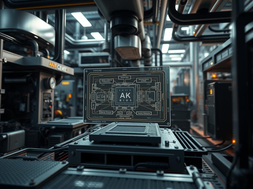
The engineering design of UEFI bios rom capacity relies on the partitioning of the SPI flash into several distinct regions: the Descriptor Region, the GbE (Gigabit Ethernet) Region, the ME (Management Engine) or CSME (Convergent Security and Manageability Engine) Region, and the BIOS Region itself. The UEFI BIOS Region is further subdivided into Firmware Volumes. The logic behind this design is to provide an idempotent boot process where the hardware state can be reliably reproduced regardless of previous system crashes. We apply encapsulation to various Driver Execution Environment (DXE) modules to ensure that the payload delivered to the CPU is both secure and structured. By managing the UEFI NVRAM space effectively, we minimize signal-attenuation risks during high-frequency data transfers across the SPI bus.
Step-By-Step Execution
1. Identify the Flash Controller and Chip ID
Run the command flashrom –programmer internal to probe the system for the existing SPI controller. This action queries the PCH (Platform Controller Hub) to identify the specific hardware ID of the flash chip.
System Note: This step initializes the SPI interface kernel driver, allowing the operating system to map the physical memory address of the BIOS ROM to a virtual memory space for direct access.
2. Extract the Current ROM Image for Analysis
Execute flashrom -p internal -r backup_bios.bin to create a bit-perfect copy of the existing firmware.
System Note: This command performs a sequential read of the entire memory map. It is critical for establishing a recovery point should the subsequent write operation fail due to thermal-inertia on the chip pins or a sudden power loss.
3. Analyze Firmware Volume Utilization via UEFITool
Open the binary in UEFITool and navigate to the Firmware Volume (FV) section to inspect the available free space. Focus specifically on the NVRAM storage and DXE main volumes.
System Note: This tool parses the FFS (Flash File System) headers. Analyzing the uefi bios rom capacity at this level identifies if the current capacity can accommodate newer, larger microcode patches without deleting essential drivers.
4. Optimize Payload and Microcode
Use ifdtool -u backup_bios.bin to unlock the descriptor if necessary; then, use a script to replace outdated microcode files in the Microcode Binary (MCB) region.
System Note: Modifying the Intel Flash Descriptor (IFD) changes the read/write permissions at the hardware level. This ensures that the CSME does not trigger a global reset during the boot phase when it detects a signature mismatch in the BIOS region.
5. Flash Updated Image to the ROM
Deploy the optimized image using flashrom -p internal -w optimized_bios.bin.
System Note: The software sends the WREN (Write Enable) opcode to the SPI chip. The internal logic-controller of the chip then performs a sector erase followed by a page program. Failure at this step usually results from packet-loss on the management bus or incorrect voltage levels.
6. Verify Checksum and Post-Write Integrity
Execute flashrom -p internal -v optimized_bios.bin to compare the physical content of the ROM against the source file.
System Note: This performs a byte-by-byte comparison. It ensures that no bit-flips occurred during the write process; such flips are often caused by electrical noise or signal-attenuation in unshielded environments.
Section B: Dependency Fault-Lines:
The most common mechanical bottleneck in uefi bios rom capacity upgrades is the Hardware Sequencing lock implemented by modern chipsets. If the Flash Configuration Register is set to “Read-Only” by the manufacturer, software-based flashing will fail. Another significant conflict exists between the Intel Management Engine (ME) and the BIOS region; if the ME partition is corrupted during the resize of the BIOS volume, the system will enter a “Boot Loop” or shut down after 30 minutes. Library conflicts in Linux, such as missing libftdi or libpci, can also prevent the flashrom utility from communicating with external programmers.
THE TROUBLESHOOTING MATRIX
Section C: Logs & Debugging:
When a flash operation fails, the first point of reference is the system kernel log. Use dmesg | grep -i spi to look for “Status Register” errors. If the error “Transaction error!” appears, check the physical connection to the SPI pins. For UEFI-level errors, such as “Load Image Fail,” use a serial-to-USB converter connected to the RS232/UART pins on the motherboard. Monitor the serial output during POST; error codes like 0xAB or 0x55 usually indicate a failure in the PEI (Pre-EFI Initialization) phase, meaning the CPU cannot find a valid entry point in the uefi bios rom capacity.
| Error Code/String | Probable Cause | Corrective Action |
| :— | :— | :— |
| “Size mismatch” | Incorrect ROM chip target | Verify chip density with flashrom -L |
| “Verification failed” | Signal-attenuation/Noise | Shorten SPI cables or reduce bus frequency |
| “FREG0: Flash Descriptor” | Write-protected region | Use an external programmer to bypass PCH |
| “NVRAM Full” | Variable fragmentation | Clear CMOS or run SMM garbage collection |
OPTIMIZATION & HARDENING
Performance Tuning (Concurrency & Throughput): To improve boot latency, enable Quad-SPI (QSPI) mode in the firmware descriptor. This increases the throughput of the data transfer between the SPI ROM and the SRAM where the BIOS is decompressed; effectively cutting the initialization time by 50 percent compared to standard SPI.
Security Hardening (Permissions & Fail-safe Logic): Implement Intel Boot Guard or AMD Hardware Validated Boot. This technology uses a public key hash burned into the Field Programmable Fuses (FPF) of the CPU to verify the integrity of the uefi bios rom capacity. If the signature in the ROM does not match, the system will refuse to execute the reset vector, preventing unauthorized firmware execution. Ensure the BIOS_WP (Write Protect) pin is physically pulled high or controlled via a dedicated GPIO on the SIO (Super I/O) chip.
Scaling Logic: In large-scale cloud deployments, use Redfish API or IPMI to manage uefi bios rom capacity across thousands of nodes. This allows for centralized “Fleet Updates.” Use a staggered deployment strategy to account for thermal-inertia and power-grid load, ensuring that if a specific firmware version causes a high failure rate, the incident is contained to a single rack.
THE ADMIN DESK
Q: Can I replace an 8MB ROM chip with a 16MB chip?
A: Yes, provided the pinout (usually SOP-8 or WSON-8) and voltage match. You must also update the Flash Descriptor to reflect the new density; otherwise, the system will only address the original 8MB of the uefi bios rom capacity.
Q: Why is my NVRAM space decreasing automatically?
A: UEFI systems store crash logs, boot entries, and secure boot keys in NVRAM. Over time, frequent updates or OS reinstalls create overhead through fragmented variables. Running a firmware-level garbage collection or clearing the CMOS usually restores the available payload space.
Q: What happens if the SPI bus frequency is too high?
A: Excessive frequency causes signal-attenuation and data corruption. If the traces on the PCB are not impedance-matched, high frequencies lead to reflections. This results in the CPU reading “garbage” data, causing an immediate system hang at the reset vector.
Q: Is “Dual BIOS” a solution for ROM capacity issues?
A: No; Dual BIOS provides redundancy, not increased capacity. It uses two separate physical chips with identical code. To increase actual capacity, you must utilize a higher-density chip or optimize the firmware to reduce the size of the DXE drivers.
Q: How do I identify if my ROM is 1.8V or 3.3V?
A: Check the part number on the IC surface. For example, a Winbond 25Q128FV is 3.3V, while a 25Q128FW is 1.8V. Applying 3.3V to a 1.8V chip will cause permanent thermal damage to the internal logic-gate structure.

