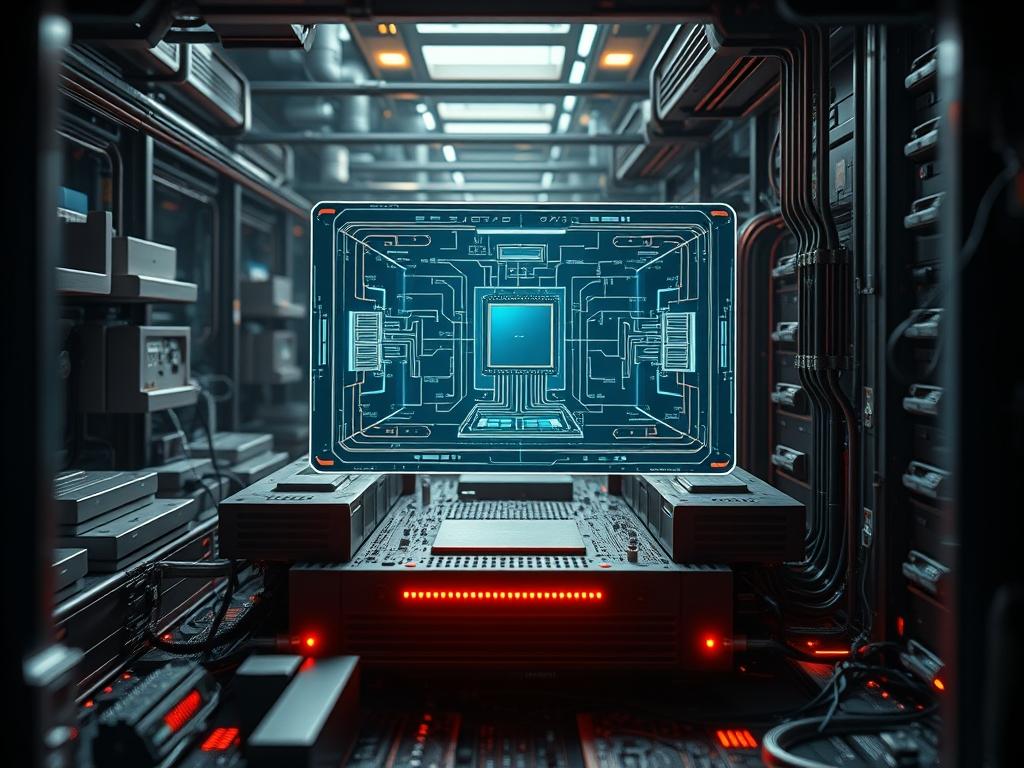
Integrating high-density motherboard pcb layers into a modern compute architecture requires an exhaustive understanding of the physical layer foundation. Within the broader technical stack of cloud and network infrastructure, the motherboard acts as the critical layer 0. It serves as the physical vessel for data transport, power regulation, and mechanical structural integrity. As signal speeds move into the multi-gigahertz range, the motherboard pcb layers transition from simple electrical interconnections to complex transmission lines where signal-attenuation and electromagnetic interference (EMI) become the primary architectural bottlenecks. The problem facing systems architects is the inherent physics of signal degradation over long trace lengths and high-frequency switching. The solution resides in the strategic deployment of high-layer density and sophisticated shielding methodologies. By utilizing a multi-layered stackup, architects can provide dedicated return paths for high-speed signals, effectively using ground and power planes to create a Faraday cage effect. This technical manual details the parameters required to maintain signal integrity and thermal stability in mission-critical hardware deployments.
Technical Specifications
| Requirement | Default Operating Range | Protocol/Standard | Impact Level (1-10) | Recommended Resources |
| :— | :— | :— | :— | :— |
| Layer Count | 6 to 16 Layers | IPC-2221B | 10 | High Tg FR4 or Rogers 4350B |
| Trace Impedance | 50 to 100 Ohms (+/- 10%) | IEEE 802.3ck | 9 | impedance_calculator_v2.1 |
| Copper Weight | 1.0oz to 2.0oz (Outer) | IPC-6012 | 7 | thermal_sink_density |
| Dielectric Constant | 3.5 to 4.5 Dk | IEC 61189-2 | 8 | Low-loss Dielectric Material |
| Min. Via Size | 0.1mm to 0.3mm | IPC-T-50 | 6 | Laser Drill / Microvia |
| Thermal Conductivity | 0.25 to 3.5 W/mK | ISA-S71.04 | 9 | Active Liquid Cooling/Airflow |
The Configuration Protocol
Environment Prerequisites:
Before finalizing the motherboard pcb layers design, the environment must meet the following technical criteria:
1. Full compliance with IPC-A-600 (Acceptability of Printed Boards) and IPC-6012 (Qualification and Performance Specification for Rigid Printed Boards).
2. Electronic Design Automation (EDA) software such as Altium Designer or Cadence Allegro must be updated to the latest stable release to ensure the geometric kernels handle 0.1 micron precision.
3. Designers must have read/write permissions to the design_rule_check (DRC) library files and the layer_stack_manager variables within the enterprise PLM system.
4. Standard reference environment: 20 degrees Celsius, 45% relative humidity to minimize electrostatic discharge (ESD) during physical audit.
Section A: Implementation Logic:
The engineering logic behind high-density motherboard pcb layers is centered on the principle of controlled impedance and signal encapsulation. In a standard 8-layer stackup, signals are routed through a “stripline” or “microstrip” configuration. Stripline routing places the signal trace between two reference planes (Ground or Power), which provides superior EMI shielding and reduces signal-attenuation. This design choice is necessitated by the high-speed PCIe_Gen_5 and DDR5 interfaces, where even minor variations in the dielectric constant (Dk) can lead to significant latency and packet-loss. By increasing the layer density, we essentially create an idempotent environment where the electrical properties remain consistent across the entire surface of the board, regardless of the concurrency of high-speed data bursts. Furthermore, thicker copper on the internal layers increases the thermal-inertia of the system, allowing the motherboard to absorb sudden spikes in TDP from the CPU and GPU without immediate mechanical stress or delamination of the substrate.
Step-By-Step Execution
1. Define the Master Layer Stackup
Access the Layer Stack Manager in your EDA utility and define the vertical arrangement of copper and dielectric materials. Ensure that every signal layer is immediately adjacent to at least one reference ground plane.
System Note: This action defines the physical impedance of the traces; a failure to align signal layers with ground planes will result in high return-current loops, causing the kernel to report PCIe_Bus_Error or Correctable_Error_Count spikes in dmesg.
2. Configure Differential Pair Constraints
Establish the diff_pair_routing_rules within the software to maintain a constant 90-ohm or 100-ohm impedance for high-speed protocols. Use a fluke-multimeter and a Time Domain Reflectometer (TDR) to verify the physical prototypes against the digital twin.
System Note: Correct differential routing minimizes the payload distortion. If traces are not length-matched within 0.005 inches, the hardware-level timing sync will fail, forcing the NIC or storage controller into a lower-speed fallback mode or increasing latency.
3. Implement Via Stitching and Shielding
Deploy a grid of ground vias (Via Stitching) around the board perimeter and near high-frequency components to create a low-impedance path to the ground. Use systemctl status sensors to monitor the impact of heat dissipation as you adjust the via density.
System Note: Via stitching acts as a mechanical and electrical stabilizer for the kernel’s power management subsystem. It reduces the ground-bounce effect, ensuring that the V_core voltage remains stable during high CPU throughput scenarios.
4. Optimize the Power Delivery Network (PDN)
Assign wide copper pours for the Power_Planes to handle the high amperage required by the voltage regulator modules (VRMs). Verify the plane integrity by checking for “Swiss Cheese” effects caused by excessive via penetrations.
System Note: A solid PDN ensures the system can handle massive concurrency in multi-threaded applications. If the PDN is poorly architected, the OS may experience random reboots or “Kernel Panic: Power Loss” despite the PSU providing adequate total wattage.
Section B: Dependency Fault-Lines:
During the fabrication and audit of motherboard pcb layers, several mechanical and electrical bottlenecks frequently occur:
- Impedance Mismatch: If the fabrication house uses a dielectric material with a different Dk than specified in the config_file, the impedance will shift. This causes signal reflections that look like “noise” to the logical layer, leading to high packet-loss.
- Via Stub Resonance: Unused portions of vias (stubs) can act as antennas, radiating EMI. This requires “back-drilling” to remove the excess copper, a process that adds to the manufacturing overhead but is essential for 112G signal paths.
- Thermal Expansion: Dissimilar materials have different Coefficients of Thermal Expansion (CTE). Under high thermal-inertia, the layers can shear, breaking internal connections and causing an intermittent “No Boot” condition that is difficult to replicate in a lab.
THE TROUBLESHOOTING MATRIX
Section C: Logs & Debugging:
When diagnosing motherboard pcb layers failures, start at the physical layer and move toward the firmware logs.
- Error Code 0x00000124 (WHEA_UNCORRECTABLE_ERROR): Often indicates a hardware-level failure in the signal path. Verify the PCIe_Link_Status in the BIOS/UEFI. If the width shows x4 instead of x16, check for physical contamination in the PCB layers near the slot.
- TDR Waveform Analysis: Use a TDR to scan the trace path. A sudden spike in the waveform indicates an open circuit (crack in the PCB layer); a sudden dip indicates a short circuit.
- Log Path /var/log/mcelog: In Linux environments, use mcelog to decode Machine Check Exceptions. Look for “Bus error/Data parity” strings which point specifically to memory traces on the inner layers of the PCB.
- Visual Cue (Moiré Patterns): Under X-ray inspection, Moiré patterns in the copper mesh indicate misalignment during the lamination process, which correlates with intermittent data corruption under high load.
OPTIMIZATION & HARDENING
- Performance Tuning: To maximize throughput, ensure that high-speed traces are routed on the layers furthest from the external surfaces (internal layers 3, 5, 8, etc.) to benefit from the natural encapsulation of the ground planes. This reduces the overhead of error-correction protocols.
- Security Hardening: On mission-critical motherboards, “buried” vias (vias that do not reach the surface) can be used to prevent physical probing of sensitive data buses, such as those carrying encryption keys between the CPU and the TPM.
- Scaling Logic: When moving from an 8-layer to a 12-layer or 16-layer design, always maintain a symmetrical stackup. An asymmetrical stackup will cause the board to warp during the soldering process, leading to mechanical stress on BGA (Ball Grid Array) components and eventual solder joint failure.
THE ADMIN DESK
How do I detect internal layer delamination?
Perform a visual inspection for “measling” (small white spots under the surface) or use a thermal camera while the system is under load. Hotspots in areas without active components often indicate internal shorts between motherboard pcb layers.
What is the impact of a 10% impedance variance?
A 10% variance is generally acceptable for signals under 1GHz. However, for Gen 5 PCIe or 100G Ethernet, this variance can cause significant signal-attenuation and trigger frequent re-transmission of data, reducing your overall system throughput by up to 30%.
Can I repair a broken internal PCB trace?
Rarely. If an internal layer trace is severed, the “Quick-Fix” involves bypassing the internal path with a micro-coaxial jumper on the surface. This is a temporary measure and usually violates EMI compliance standards.
What does “copper thieving” do for my motherboard?
Copper thieving involves adding non-functional copper dots to empty areas of the motherboard pcb layers. This ensures even plating thickness during manufacturing, which prevents the board from bowing and keeps the trace geometry within technical specifications.
How does layer count affect thermal-inertia?
Higher layer counts, specifically those with more internal ground planes, increase the board’s mass and thermal-inertia. This allows the motherboard to act as a primary heatsink, slowing the rate of temperature increase during bursty compute workloads.

